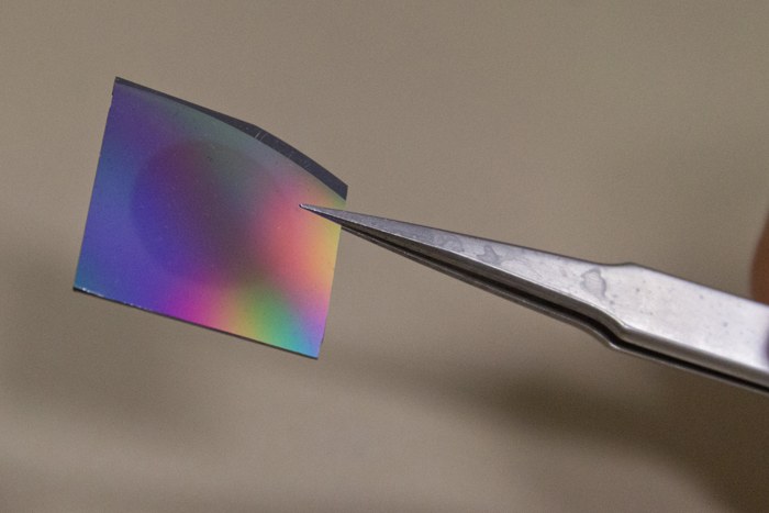
A breakthrough for the advanced microelectronics and photovoltaic sectors
Jun 13, 2013
UPC researchers have discovered a technique to produce cheaper and more flexible multiple thin crystalline silicon wafers.
A team of researchers from the Nanoengineering Research Centre (CRNE) and the Department of Electronic Engineering at the UPC has found a way to make the manufacture of crystalline silicon materials faster and more affordable. The results of their research have recently been published in the online version of the landmark journal Applied Physics Letters.
Thin crystalline silicon wafers measuring around 10 µm (micres) are costly but also very sought after in the field of microelectronics, especially in view of the growing demand for 3D circuit integration with microchips. Silicon wafers also have potential photovoltaic applications in the medium term in the conversion of sunlight to electricity and the production of more affordable, more flexible and lighter solar cells.
+ Info

Share: